Developer Manual/Super IO
The wiki is being retired!
Documentation is now handled by the same processes we use for code: Add something to the Documentation/ directory in the coreboot repo, and it will be rendered to https://doc.coreboot.org/. Contributions welcome!
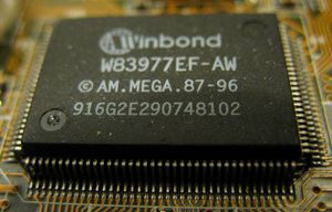
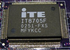
The Super I/O is a chip found on most of today's mainboards which is — among other things — responsible for the serial ports of the mainboard (e.g. COM1, COM2). This chip is usually the first thing you'll want to support, as it's required to get serial debugging output from the mainboard (via a null-modem cable and the proper software, e.g. minicom or CuteCom).


Super I/O bringup
Adding support for a new Super I/O chip is usually not significantly hard once you have obtained the datasheet for your target chip. Herein we shall outline the steps usally taken for a bringup.
Source layout
Create the top-level directory src/superio/vendor/device (e.g. src/superio/winbond/w83627ehg). Within src/superio/vendor edit both Kconfig and Makefile.inc the changes will be self-evident. All super i/o support is then contained in src/superio/vendor/device, we provide here the minimum of a usual bringup.
Makefile.inc
The src/superio/vendor/device/Makefile.inc should contain the following two lines:
 romstage-$(CONFIG_SUPERIO_VENDOR_DEVICE) += early_serial.c
 ramstage-$(CONFIG_SUPERIO_VENDOR_DEVICE) += superio.c
Obviously replacing VENDOR and DEVICE respectively.
device.h, (e.g., w83627ehg.h)
The src/superio/vendor/device/device.h header should contain the Super I/O supported Logical Device Numbers (LDN) (see below) and the early_serial enabling function prototype.
For example, for f71869ad.h we have:
 #ifndef SUPERIO_FINTEK_F71869AD_F71869AD_H
 #define SUPERIO_FINTEK_F71869AD_F71869AD_H

 /* Logical Device Numbers (LDN). */
 #define F71869AD_FDC 0x00»       /* Floppy */
 #define F71869AD_SP1 0x01»       /* UART1 */
 #define F71869AD_SP2 0x02»       /* UART2 */
 #define F71869AD_PP 0x03»       /* Parallel port */
 #define F71869AD_HWM 0x04»       /* Hardware monitor */
 #define F71869AD_KBC 0x05»       /* PS/2 keyboard and mouse */
 #define F71869AD_GPIO 0x06»       /* General Purpose I/O (GPIO) */
 #define F71869AD_BSEL 0x07»       /* BSEL */
 #define F71869AD_PME 0x0a»       /* Power Management Events (PME) and ACPI */

 void f71869ad_enable_serial(device_t dev, u16 iobase);

 #endif /* SUPERIO_FINTEK_F71869AD_F71869AD_H */
early_serial.c
The src/superio/vendor/device/early_serial.c file will be responsible to setup a serial port on the mainboard as to get serial debugging output. N.B. This will work even before the RAM is initialized, thus is useful/required for debugging the RAM initialization process. In this file you now declare a function device_enable_serial() which enables the requested serial port. For example:
 void w83627ehg_enable_serial(device_t dev, unsigned int iobase)
 {
        pnp_enter_ext_func_mode(dev);
        pnp_set_logical_device(dev);
        pnp_set_enable(dev, 0);
        pnp_set_iobase(dev, PNP_IDX_IO0, iobase);
        pnp_set_enable(dev, 1);
        pnp_exit_ext_func_mode(dev);
 }
where we defined the functions prototype in the src/superio/vendor/device/device.h as to link it into both the rom and ram stages. We also must statically declarate two helper functions:
 /*
  * Enable configuration: pass entry key '0x87' into index port dev.
  */
 static void pnp_enter_conf_state(device_t dev)
 {
 »       u16 port = dev >> 8;
 »       outb(0x87, port);
 »       outb(0x87, port);
 }

 /*
  * Disable configuration: pass exit key '0xAA' into index port dev.
  */
 static void pnp_exit_conf_state(device_t dev)
 {
 »       u16 port = dev >> 8;
 »       outb(0xaa, port);
 }
These two procedures are what put the Super I/O chip into configuration mode and then return it back again.. N.B. The values of 0x87 and 0xAA for enable and disable configuration respectively are typical although check the Super I/O data sheet to be sure. N.B. The default index port and data port are either 0x4E and 0x4F or 0x2E and 0x2F respecively, once again check the data sheet.
- Whether the Super I/O is at config address 0x2e (the usual case) or 0x4e (or some other address) is mainboard-dependent. You can find out the address by running superiotool.
This value is usually defined in the mainboards devicetree.cb file under the pnp device in any case.
Mainboards which have this Super I/O chip, will call this function in their romstage.c file. Example:
 #include "superio/winbond/w83627ehg/w83627ehg.h"
 [...]
 #define SERIAL_DEV PNP_DEV(0x2e, W83627EHG_SP1)
 [...]
 w83627ehg_enable_dev(SERIAL_DEV, TTYS0_BASE);
 uart_init();
 console_init();
superio.c
While writing the superio.c part of the Super I/O bring up you will encounter the data structure static struct pnp_info pnp_dev_info[] = {} to prepare. The following information may help to understand the LDN mask pairing:
/*
 * io_info contains the mask 0x07f8. Given 16 register, each 8 bits wide of a
 * logical device we need a mask of the following form:
 *
 *  MSB                 LSB
 *    v                 v
 * 0x[15..11][10..3][2..0]
 *    ------  ^^^^^  ^^^^
 *     null     |      |
 *              |      +------ Register index
 *              |
 *              +------------- Compare against base address and
 *                             asserts a chip_select on match.
 *
 * i.e., 0x07F8 = [00000][11111111][000]
 *
 */
Virtual logical devices
Some Super I/Os use register 0x30 of one logical device number (LDN) for more than one function enable. For example, it can be used to enable some GPIOs, GAME, MIDI etc. To overcome this issue a concept of virtual LDN has been introduced. Virtual LDNs can be used in coreboot to map the enable bit position in register 0x30 to virtual LDN, which will just enable the functionality map to that bit.
Original LDN always just switch on or off bit0 of register 0x30. Virtual LDN is created as follows. Low [7:0] bits are used to describe the original LDN. High [10:8] bits select the position of the bit enable in the register 0x30.
If LDN is 0x7 it will handle bit0 of register 0x30. If the (virtual) LDN is 0x107 it will handle bit1 of same register etc.