Developer Manual
The wiki is being retired!
Documentation is now handled by the same processes we use for code: Add something to the Documentation/ directory in the coreboot repo, and it will be rendered to https://doc.coreboot.org/. Contributions welcome!
Introduction
This manual is intended for aspiring coreboot developers to help them get up to speed with the code base and the tasks required to add support for new chipsets, devices, and mainboards. It currently covers coreboot v2, but will be extended to also cover the development version coreboot v3 later.
Required hardware and software tools for developers
Before starting to work on coreboot support for a new mainboard and/or chipset you'll want a few development tools (both hardware and software). Not all of them are strictly required, a lot depends on your specific task and needs.
Basic requirements
- A mainboard you want to port coreboot to.
- Datasheets
- A Linux/UNIX machine for development purposes
- The coreboot build environment is not well-supported on Windows. It may be possible to do it under cygwin but nobody has tried.
It's also handy to have one/some/all of the following:
PLAICE: Programmer, Logic Analyzer and In-Circuit Emulator
The PLAICE is a powerful in circuit development tool that combines the features of programming and emulating FLASH devices as well as high speed multi-channel logic analysis into one device.
The FLASH BIOS emulator feature will help speed development of coreboot porting since the developer will no longer have to wait for either swapping FLASH devices or for lengthy FLASH programming cycles.
The design will also perform as a multi-channel logic analyzer with a JAVA client.
The PLAICE will make use of an adapter cable that will interface to the mainboard via the FLASH BIOS socket or onto the pins of a soldered in place FLASH device. It may also be used to program a FLASH device or emulate a FLASH device in circuit. Since the PLAICE attaches directly to the in-circuit FLASH device, the FLASH may be programmed without the need to reverse engineer any FLASH WRITE/ENABLE "security through obscurity" protection schemes incorporated into a mainboard.
See also: Slashdot: An Open Source Hardware Development Tool.
Artecgroup programmable LPC dongle
PC Engines lpc1A
This board is most useful if you are working on machines from the ALIX family, but could also be useful if you can expose an LPC header on another board.
External EPROM/Flash programmer that can program the flash chip on your motherboard
External programmers are not always necessary. Use your mainboard as a programmer instead. Boot up with a known-good image, then unplug the (DIP32, PLCC32, or DIP8) ROM chip while powered on. Reflash that secondary piece and try a reboot. Many boards allow for more than one type of flash to be programmed, but clearly are less versatile than real programmers.
- Willem Universal EPROM Programmer: DOS, Windows software, work has started on Linux drivers, quite many types of EEPROM asf. ~ 35
- IDE adapter for PLCC32 & DIP32 sockets: Has Linux 2.4 & 2.6 drivers $/ ~48 (kit 33) free manual with schematics & component list downloadable (component cost approx. 5)
- GALEP-4: Has beta Linux drivers ~$300. See Galep IV for a description on how to get the more modern Windows software working in Linux with wine.
BIOS Savior

The BIOS Savior is a tool that plugs into and replaces the original mainboard Flash device. The BIOS Savior has its own Flash device and a socket for the original mainboard Flash device (PLCC or DIP versions are available). It features a switch to allow the developer to choose between which Flash device is accessed by the mainboard during read and write cycles.
This device helps to minimize the amount of hot swapping required and reduces mechanical and electrical stress on the BIOS chips.
The BIOS Savior is available from:
Top Hat Flash
A similar function is achieved by the "top hat flash" which comes at no extra cost with many Elitegroup, and some Gigabyte and Albatron mainboards like ECS KN3 SLI2 Extreme with MCP55 southbridge (which is getting severely out of stock around central europe as of 8/2007 unfortunately). After bootup, it can manually be lifted off the original BIOS chip, so the original BIOS can be reflashed after a failure. /rst is wired to /oe on the spare chip otherwise 1:1. Top hat flash is equipped with a Winbond W39V040AP FWH. It may rely on particular circuitry on the mainboard to operate.

Chip removal tools
If you're hot-swapping your BIOS chips (i.e., removing the chip while your computer is running, then inserting another one) you'll usually need some tools.
There are different tools for DIP and PLCC chips (see photos). You can find them in most electronics stores, usually. Both types cost roughly 5-10 Euros.
Another very nifty idea is clipping off the needle point of normal office push pins, and then attaching them to (PLCC) ROM chips with super glue. That makes it pretty easy to insert and remove the ROM chips without extra tools.
Since after bootup, flash mem is not accessed anymore, you can even hot plug (plug in and out while PC powered on) push pin flashes. This way you save an external EEPROM programmer and mimic the procedure of top hat flash. Make sure you do not short circuit anything, though.
-
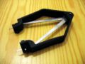
PLCC32 BIOS removal tool.
-
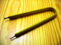
DIP32 BIOS removal tool.
-

Push pins with cut off needles, attached to ROM chips with super glue.
-
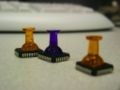
More push pins on ROM chips.


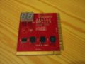
POST card
A POST card will save your life: it's the only output device (beside beeper) you have during the boot process. The term POST means Power On Self Test and comes from the original IBM specifications for the BIOS. Port 80 is a pre-defined I/O port to which programs can output a byte. The POST card displays the byte in hex on its 2 digit display. We use a lot of POST codes in coreboot, so if you can tell us the POST code you see, we will have some idea of what happened.
If your coreboot machine is working properly, you will see it count up from 0xd0 to 0xd9 (while it is gunzipping the kernel) and then display 0x98 (Linux idle loop). There are POST cards with ISA bus, PCI bus, USB und parallel port connectors (the latter for laptops).
Often they carry status LEDs for ISA/PCI signals such as: IRDY, BIOS-access, FRAME, OSC, PCI-CLK, RESET, 12V, -12V, 5V, -5V, 3.3V. Some cards were known to not function because the mainboard switches off the CLK on their slot after non-standard registration on PCI.
-
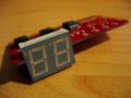
BIOS POST card for PCI.
-
BIOS POST card for PCI and ISA.


PCI POST cards can be found in various places.
See also How can I write to port 0x80 from userspace.
- http://siliconkit.dnsalias.com/cart/index.tpcip.html
- http://www.elstonsystems.com/prod/pc_analyzer.html
- http://shopv2.elstonsystems.com/product_info.php/products_id/57
- http://www.uxd.com/trio.html
- http://www.soyousa.com/products/proddesc.php?id=261
Null-modem cable
A so-called null-modem cable is used for transmitting the output from a serial coreboot (or GRUB- or Linux-) console to another computer where a terminal program (such as minicom) can be used to display/save the messages.
-
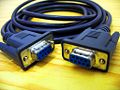
A null-modem cable.

Compact Flash IDE adaptor
Solid state disks (e.g. CompactFlash cards) save time during the repeated boot process compared with regular hard disks.
- http://siliconkit.dnsalias.com/cart/index.tcfdp.html
- http://www.cwlinux.com/eng/products/products_ide2cf.php
- http://www.mini-box.com/s.nl/sc.8/category.14/.f
- http://www.acscontrol.com/Index_ACS.asp?Page=/Pages/Products/CompactFlash/IDE_To_CF_Adapter.htm
- http://www.pcengines.ch/cflash.htm
- http://www.psism.com/adcf.htm
- http://www.hsc-us.com/industrial/adapter/ATP.html (2xCF, one with hotswap!)
- http://www.mesanet.com/ (Choose DISK EMULATORS then CFADPTHD in the menu. 2xCF)
Oscilloscope
For hardware debugging purposes when it goes down the most atomic details. Consider logic analyzers as alternative.
In Circuit Emulator hardware debugger
Allows very time-saving burn/debug cycles with added tracing capabilities but somewhat costly.
coreboot SDK
In Circuit chip programmer
Should allow you to program your BIOS even if it is soldered to the motherboard.
EPROM emulators
These hardware devices pretend to be an EEPROM chip.
- http://www.tech-tools.com/romtools.htm
- http://xtronics.com/memory/pktROM.htm
- http://www.tribalmicro.com/multirom/
- http://www.linuxselfhelp.com/HOWTO/Diskless-HOWTO-10.html (a larger list -- outdated)
USB debug devices

An alternative to a serial console may be a USB debug device. They are not so common, yet. Their advantage is higher speed than a serial console. One might hook an FPGA to it for profiling purposes or some automated checks. Accessing a USB debug device from within BIOS is not different than other USB devices, and is part of the USB standard.
See also EHCI Debug Port.
Hardware Overview
Intel Architecture
Hardware Reset
|
The first instruction that is fetched and executed following a hardware reset is located at physical address 0xFFFFFFF0. This address is 16 bytes below the processors uppermost physical address. The EPROM containing the software-initialization code must be located at this address. The address 0xFFFFFFF0 is beyond the 1-MByte addressable range of the processor while in real-address mode. The processor is initialized to this starting address as follows. The CS register has two parts: the visible segment selector part and the hidden base address part. In real-address mode, the base address is normally formed by shifting the 16-bit segment selector value 4 bits to the left to produce a 20-bit base address. However, during a hardware reset, the segment selector in the CS register is loaded with 0xF000 and the base address is loaded with 0xFFFF0000. The starting address is thus formed by adding the base address to the value in the EIP register (that is, 0xFFFF0000 + 0xFFF0 = 0xFFFFFFF0). The first time the CS register is loaded with a new value after a hardware reset, the processor will follow the normal rule for address translation in real-address mode (that is, [CS base address = CS segment selector * 16]). To insure that the base address in the CS register remains unchanged until the EPROM based software-initialization code is completed, the code must not contain a far jump or far call or allow an interrupt to occur (which would cause the CS selector value to be changed). |
FWH/LPC Flash Memory
Modern mainboards are often equipped with Firmware Hub (FWH) or Low Pin Count (LPC) flash memory used to store the system bootloader ("BIOS"). Execution begins by fetching instructions 16 bytes below the flash memory's uppermost physical address.
coreboot Overview
View From The CPU: Intel Architecture
- at
0xFFFFFFF0, start execution atreset_vectorfrom src/cpu/x86/16bit/reset16.inc, which simply jumps to_start _startfrom src/cpu/x86/16bit/entry16.inc, invalidates the TLBs, sets up a GDT for selector 0x08 (code) and 0x10 (data), switches to protected mode, and jumps to__protected_start(setting the CS to the new selector 0x08). The selectors provide full flat access to the entire physical memory map.__protected_startfrom src/cpu/x86/32bit/entry32.inc, sets all other segment registers to the 0x10 selector- execution continues with various
mainboardinitfragments:__fpu_startfrom cpu/x86/fpu/enable_fpu.inc(unlabeled)from cpu/x86/sse/enable_sse.inc- some CPUs enable their on-chip cache to be used temporarily as a scratch RAM (stack), e.g. cpu/amd/model_lx/cache_as_ram.inc
- the final
mainboardinitfragment is mainboard-specific, in 'C', called auto.c (or cache_as_ram_auto.c). It is compiled with 'romcc', and it includes and uses other C-code fragments for:- initializing MSRs, MTTRs, APIC
- setting up the Southbridge minimally ("early setup")
- setting up SuperIO serial
- initializing the console
- initializing RAM controller and RAM itself
- execution continues at
__mainfrom src/arch/i386/init/crt0.S.lb, where the non-romcc 'C' coreboot code is copied (possibly decompressed) to RAM, then the RAM entry point is jumped to. - the RAM entry point is
_startarch/i386/lib/c_start.S, where new descriptor tables are set up, the stack and BSS are cleared, the IDT is initialized, andhardwaremain( )is called (operation is now full 32-bit protected mode 'C' program with stack) hardwaremain( )is from boot/hardwaremain.c, the console is initialized, devices are enumerated and initialized, configured and enabled- the payload is called, either via
elfboot( )from boot/elfboot.c, orfilo( )from boot/filo.c
Memory map
On x86 systems, many memory ranges are reserved for special purposes or have some other peculiar properties. The article Memory map has details about this fact.
Serial output and the Super I/O
The Super I/O is a chip found on most of today's mainboards which is — among other things — responsible for the serial ports of the mainboard (e.g. COM1, COM2). This chip is usually the first thing you'll want to support, as it's required to get serial debugging output from the mainboard (via a null-modem cable and the proper software, e.g. minicom or CuteCom).


The steps for adding support for a new Super I/O chip are:
- Add a directory src/superio/vendor/device (e.g. src/superio/winbond/w83627ehg).
- In that directory, add a file device_early_serial.c (e.g. w83627ehg_early_serial.c). This file will be responsible to setup a serial port on the mainboard so that you can get serial debugging output. This will work even before the RAM is initialized, thus is useful/required for debugging the RAM initialization process.
- In this file you now declare a function device_enable_serial() which enables the requested serial port. Example:
 static void w83627ehg_enable_serial(device_t dev, unsigned int iobase)
 {
        pnp_enter_ext_func_mode(dev);
        pnp_set_logical_device(dev);
        pnp_set_enable(dev, 0);
        pnp_set_iobase(dev, PNP_IDX_IO0, iobase);
        pnp_set_enable(dev, 1);
        pnp_exit_ext_func_mode(dev);
 }
- Mainboards which have this Super I/O chip, will call this function in their auto.c or cache_as_ram_auto.c file. Example:
 #include "superio/winbond/w83627ehg/w83627ehg_early_serial.c"
 [...]
 #define SERIAL_DEV PNP_DEV(0x2e, W83627EHG_SP1)
 [...]
 w83627ehg_enable_dev(SERIAL_DEV, TTYS0_BASE);
 uart_init();
 console_init();
- Whether the Super I/O is at config address 0x2e (the usual case) or 0x4e (or some other address) is mainboard-dependent. You can find out the address by running superiotool.
Virtual logical devices
Some Super I/Os use register 0x30 of one logical device number (LDN) for more then one function enable. For example, it can be used to enable some GPIOs, GAME, MIDI etc. To overcome this issue a concept of virtual LDN has been introduced. Virtual LDNs can be used in coreboot to map the enable bit position in register 0x30 to virtual LDN, which will just enable the functionality map to that bit.
Original LDN always just switch on or off bit0 of register 0x30. Virtual LDN is created as follows. Low [7:0] bits are used to describe the original LDN. High [10:8] bits select the position of the bit enable in the register 0x30.
If LDN is 0x7 it will handle bit0 of register 0x30. If the (virtual) LDN is 0x107 it will handle bit1 of same register etc.
Northbridge
RAM init
One of the most important tasks of coreboot is to initialize your system RAM.
SDRAM
There are a number of steps you have to perform to properly initialize SDRAM. This depends on the chipset, as well as the DIMMs which are inserted into the mainboard (and their properties, such as CAS latencies, and so on).
Sample northbridge datasheets:
- http://support.intel.com/design/chipsets/810/
- http://support.intel.com/design/chipsets/datashts/290656.htm
- http://download.intel.com/design/chipsets/datashts/29065602.pdf
Sample SDRAM datasheets:
- http://www.micron.com/products/partdetail?part=MT48LC16M16A2BG-75
- http://download.micron.com/pdf/datasheets/dram/sdram/256MSDRAM.pdf
DDR
DDR2
DDR3
Resources
SDRAM:
- Intel SPD Standard
- Micron 512 MB SDRAM Datasheet (PDF) -- contains some helpful explanations
DDR SDRAM:
- JEDEC DDR SPD Standard (PDF)
- Understanding DDR Serial Presence Detect (SPD) Table
- Micron DDR400 Datasheet
DDR2 SDRAM
DDR3 SDRAM
Note: Micron lists SPD values for all the memory they produce. This really helps when trying to trouble shoot memory and SPD values. Micron SPD Lookup
Southbridge
Mainboard
Config.lb
The mainboard config.lb contains many build and platform configuration settings. One of the most important items is the mainboard device list.
A device needs to be listed in the mainboard config.lb if it requires more setup than standard PCI initialization (resource allocation). Typically, that includes the CPU, northbridge, southbridge, and SIO. These devices are usually required for system specific configuration as well as indicate the system bus structure (pci_domain).
When a device in config.lb is found during the coreboot PCI/system scan process the functions to do customized initialization are called via the device_operations and the chip_operations structures. You will find these structures in the devices source files.
Options.lb
irq_table.c
Creating a new Target
To create a new mainboard target you have to add several files.
- Multiple files in src/mainboard/vendorname/mainboardname (replace vendorname and mainboardname, of course).
- A file targets/vendorname/mainboardname/Config.lb which specifies a few target-specific config options, e.g. the ROM chip size, the payload, etc.
Miscellaneous Tips
minicom
Minicom is not just a serial terminal. It was written long before the internet existed and electronic communication was only possible with a modem to a mailbox-computer. Minicom is written with the ncurses library and provides its magic via a text interface. Other than logging, it provides z-modem up- and download-capability.
CuteCom
This is an easy to use serial-terminal-program which is even able to write all communication into a log-file. It needs a computer with installed Qt-libs.

Documentation and datasheets
Useful hardware/concepts documentation for developers
These external documents and slides explain fundamental concepts of hardware that coreboot supports.
Interrupts
- PCI Interrupts on x86 machines from John Baldwin
- PCI IRQ Routing on a Multiprocessor ACPI System at Microsoft's Windows Hardware Developer Central
System Managment Mode
- System Managment Mode Overview by Robery R. Collins
Specific datasheets
TODO.

|
This work is free software; you can redistribute it and/or modify it under the terms of the GNU General Public License as published by the Free Software Foundation; either version 2 of the License, or any later version. This work is distributed in the hope that it will be useful, but WITHOUT ANY WARRANTY; without even the implied warranty of MERCHANTABILITY or FITNESS FOR A PARTICULAR PURPOSE. See the GNU General Public License for more details. |